Components
Components (library devices) are the heart of every schematic. A component is much more than a drawing on the sheet: it connects the symbol you see, the parameters you can change, the netlist used for simulation, and the layout created by schematic-driven layout.
Think of a component as a complete “device card” in a library. When you place that card on a schematic, the SchematicEditor knows how it looks, how it is named, how it is simulated, and how its silicon or PCB footprint should be built.
Almost everything about a component is edited in Edit Component. Choose the component in the library list, then open Edit Component. Full native editing is available for LayoutEditor libraries (.lel). Other library formats can often be imported into this dialog; after import, save as .lel if you want to keep all LayoutEditor options. Technical details of the file format are described under LEL.
Important: the small “+” button
When Edit Component first opens, some controls are hidden so the dialog stays simple. Press the small + button to show:
- Import and Delete
- component is a link (link to ground, port, or another component)
- several symbols for one component (symbol number)
- the Extraction tab
If you cannot find a feature mentioned below, press + first.
Library Info (whole library)
Besides editing single components, you can open Library Info for the selected library (library panel).
There you see:
- library name, type (for example
lel), file, path - how many components it contains
- whether the file is writable
For writable .lel libraries you can also edit:
Info text for the whole library
A free text field for notes about the library: who maintains it, which process it is for, version remarks, and so on. This text is stored once for the library (not per component) and is useful for teams and PDKs.
Filters (categories)
Filters are named groups of components (for example “resistors”, “digital”, “ESD”). They appear in the library filter UI so users can find devices faster.
- Add… / Remove / Rename… manage filter names
- Select a filter, then check which components belong to it
Only .lel libraries that are writable can be changed here. Other library types show the information read-only.
Edit Component — General
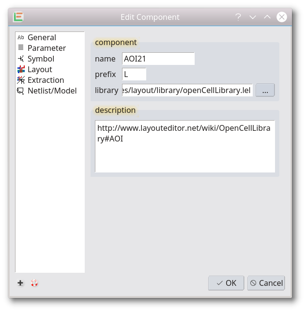
Name, prefix, library, description
- Component name — the type name used when the device is placed (for example
INV,nmos,R_poly). - Prefix — letters used at the start of instance names (for example
R→R1,R2;M→M1). - Library — which library file this component belongs to. To move a component, change the library name/path. For OpenAccess, use a name ending in
.oa(for examplemyLib.oa). - Description — text for users. If it contains a web address (http…), Component Info may open that page in a browser instead of only showing a message box.
Component is a link (after pressing +)
Sometimes a library entry should not be a full device definition, but a shortcut to something else. Enable component is a link and choose:
- ground — placing this entry places a ground
- port — placing this entry places a port
- component — placing this entry places another real component; enter that component’s cell name and library
Links still keep their own prefix/parameters in the library entry, but the placed object follows the link target. This is useful for tidy PDK palettes (aliases) without duplicating whole definitions.
Parameter
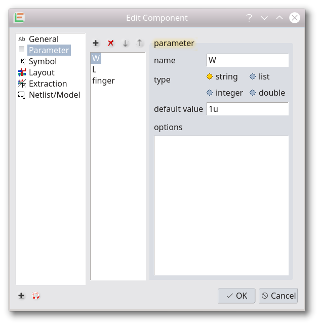
Parameters are the values a user can set on each placement (width, length, model name, package, and so on).
In the middle you see the list of parameters. Buttons above the list add, remove, and reorder them. The order in this list is the order in the parameter dialog when you edit a placed device.
Click a parameter to edit it on the right:
Parameter types
- string — free text (for example a model name or a formula)
- list — fixed choices; the user picks from a drop-down
- integer — whole numbers
- double — decimal numbers
Each parameter can have a default value. For a list, enter all allowed values.
Parameter options (one line per option)
In the options box, write lines like option=value. Supported options:
| Option | What it means in everyday language |
|---|---|
info=… |
Extra help shown as a tooltip while the user edits the value |
unit=… |
Unit shown next to the field (for example µm, kOhm) |
callback=… |
After the user changes the value, run this LayoutEditor macro or Tcl script (for checks or to update other parameters) |
edit=false |
The user cannot type the value; it is display-only (often filled by a callback) |
display=false |
The parameter is hidden in the parameter dialog |
parse=true |
Treat the value as a formula, not only as plain text (see below) |
parseAsNum=false |
Do not force the result to be treated as a number |
multiplier=true |
This parameter is a multiplicity factor m for layout / array use |
pcbPackage=true |
This parameter selects a PCB package from the package catalog (footprints), instead of a simple typed list |
Example options block:
unit=µm
info=drawn channel width
parse=true
Formulas in parameters (parse=true) — explained slowly
Without parse, the text you type is stored as-is.
With parse=true, the SchematicEditor tries to calculate the value. That is useful for parametric devices:
- You can enter
4*8and the tool uses32. - One parameter can depend on another. In a LayoutEditor macro this is often written with
iPar("name"), which means: “take the current value of the parameter called name”. - If the formula cannot be calculated, the original text is kept so nothing is silently lost.
You do not need to be a programmer to use this: in Edit Component, set the parameter type (often string or double), add the line parse=true, and enter a default like 2*w only if your flow expects that. For day-to-day PDK use, many parameters are simple numbers with a unit—and that is perfectly fine.
Symbol
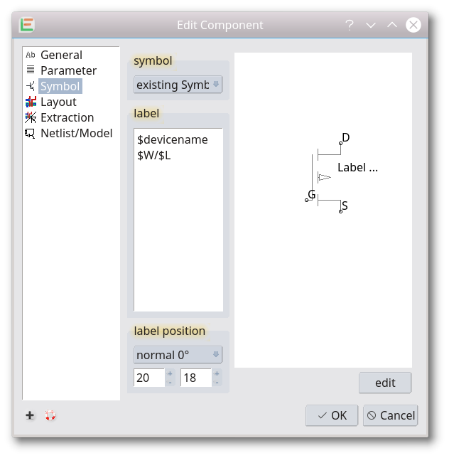
The symbol is the drawing users see on the schematic: lines, shapes, and ports (connection points).
You can:
- take a symbol from a sheet that has no components (only drawings and ports),
- open the symbol editor to draw or adjust it,
- or, if you point to a sheet that already has components, let the tool build a simple rectangle symbol from that sheet’s ports.
A symbol should contain drawing parts and ports only—not full component placements.
Label
The label is the text next to a placed device. Words that start with $ are replaced by values:
$devicename
$w/$l
nf=$nf m=$mult
model=$model
So $devicename becomes the instance name (for example M3), $w becomes the width parameter, and so on.
You can set the label position for different rotations/mirrors (0°, 90°, 180°, 270°, mirrored). Either type the offsets or Ctrl+click into the symbol preview.
Several symbols for one component (after pressing +)
Some devices need more than one drawing (for example multi-gate cells). Use the symbol number controls (shown after +) to add and select symbol slots. Each slot has its own graphics; placements can use the matching symbol.
Layout
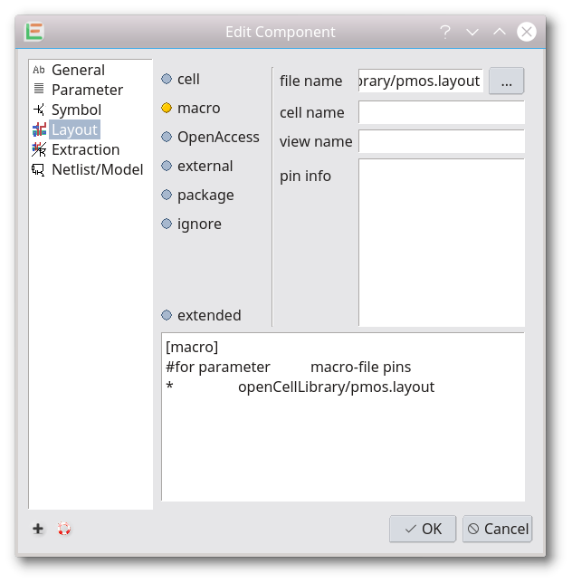
This tab answers: When schematic-driven layout runs, how should this device appear in the layout?
The tool reads the layout description from top to bottom. The first matching rule wins. Lines starting with # are comments.
On the left you choose a method (radio buttons). On the right you fill in the fields for that method—or, in extended mode, edit the full text with several methods at once.
What is a “parametric cell”?
A static layout is a fixed cell: the same shape every time (maybe chosen by a parameter such as output=X2).
A parametric cell (PCell) is different: the layout is built when needed, using the device’s parameters (width, length, fingers, …). Change w or l on the schematic, run schematic-driven layout again, and a new matching layout cell is created or reused.
In LayoutEditor, parametric layout can come from:
- a macro (LayoutEditor’s own
.layoutscripts), - Tcl including Magic (Tcl procedures / open PDK Magic-style cells),
- gdsFactory (Python gdsfactory cells),
- an external program that prints geometry,
- or OpenAccess views that already behave parametrically in your OA flow.
Below, each option is explained in plain language.
Static cell: cell
Use an existing layout cell from a file, or from the layout that is already open.
- Enter the file (or
.for “current layout”). - Enter the cell name.
- Optional pin names map connections in order.
Example idea: if parameter output is X1, use cell AND3_X1 from a GDS file; if X2, use another cell.
[cell]
# condition file cell
output=X1 openCellLibrary/AND3_X1.gds AND3_X1
output=X2 openCellLibrary/AND3_X2.gds AND3_X2
Static cell with text rewrite: package
Typical for PCB footprints. The tool loads a package cell, makes a unique copy for this instance, and rewrites texts:
- text
devicename→ the instance name - text
type→ the component type name - pin number texts → your schematic port names
Use port name nc (“not connected”) to remove a pin text you do not need.
[package]
# condition file cell port pin …
Package=SO8N pcb/SO8N.gds SO8N in+ 3 in- 2 out 6 nc 1
If a parameter is marked pcbPackage=true, the package list can come from the shipped PCB catalog.
Parametric cell: macro
A LayoutEditor macro file (usually ending in .layout) draws the cell. After the macro runs, whichever layout cell is current is used for the device.
In Edit Component choose macro, set the macro file, and optionally list pin names.
[macro]
# condition macro-file pins
* pcb/resistor.layout pin1 pin2
How the macro learns your parameters
You do not pass parameters by hand each time. When schematic-driven layout runs the macro, LayoutEditor defines values the macro can read, for example:
| Name the macro sees | Meaning |
|---|---|
NETLIST_DEVICENAME |
Instance name (for example R12) |
NETLIST_PARAMETER |
Parameter summary for this device |
NETLIST_PIN1_NAME, NETLIST_PIN2_NAME, … |
Pin names in order |
NETLIST_PATH / NETLIST_LIBRARYPATH |
Folder of the library |
NETLIST_MACROPATH |
Folder of the macro file |
Inside LayoutEditor macros, parameters are often read with iPar("parameterName")—plain meaning: “give me the value of this parameter for the current device”.
For testing a macro outside schematic-driven layout, you can put default lines at the top of the macro:
#parameter step "18.5µm"
#parameterDouble shape "0.5"
#parameterInt vertex 100
Then iPar("step") still returns a useful default when you run the macro alone. When the same macro runs as a parametric cell from the schematic, the real schematic parameter values are used instead.
Shipped examples live in libraries such as the Parametric Shape library. More API details for macros: callbacks.
Parametric cell: TCL including Magic
Choose TCL including Magic when the layout should be created by a Tcl command or procedure. This is the usual path for many open PDK flows that use Magic-style generator cells: LayoutEditor runs the Tcl side and imports the resulting geometry.
In the dialog, the file/command field holds the Tcl command to run (not necessarily a file on disk).
[tcl]
# condition TCL command
* your_pdk_draw_command here
What happens in practice:
- You set parameters on the schematic (width, length, …).
- Schematic-driven layout runs.
- LayoutEditor builds a cell name from the device type and a fingerprint of the parameters.
- If that cell already exists, it is reused. If not, the Tcl command runs and creates it.
Tcl support must be available in your LayoutEditor build. Setup of open PDK Tcl helpers is part of the PDK / Magic bridge documentation for your kit.
Parametric cell: gdsFactory
Choose gdsFactory when the layout should be created by gdsfactory (Python). LayoutEditor talks to a gdsfactory worker, asks for a named cell (a “callable”), and imports shapes and ports directly—without a manual GDS export/import round trip.
In the dialog, enter the callable, for example a path like ihp.cells.nmos (exact names depend on your PDK plugin).
[gdsFactory]
# condition callable
* ihp.cells.nmos
What you need in practice:
- gdsfactory and the PDK Python side installed as required by your kit
- PDK wiring next to the library when your flow uses a
gdsfactory.pdksetup - Parameters on the LayoutEditor component that match what the gdsfactory cell expects (names may be mapped by the PDK integration)
As with other parametric methods, results are typically cached by parameter values, so the same width/length combination reuses the same layout cell.
Static / parametric via database: OpenAccess
Loads a view from an OpenAccess library (lib / cell / view, default view often layout). Use this when your company flow stores cells in OA.
[oa]
# condition lib cell view
* pdk nmos layout
Parametric cell: external
Starts an external program. LayoutEditor passes library name, cell name, view name, and all device parameters (name=value). The program prints layout shapes as simple text lines on standard output; LayoutEditor reads that text and builds the cell.
[external]
# condition lib cell view tool
* libname cellname viewname myGenerator
Example of the text format the tool prints:
databaseunits 1.000000e-09
box 99 0 1000 1000 1600 1600
polygon 10 0 1000 1000 1200 1000 1000 1200 1000 1000
text 42 0 0 1200 1300 0 PLUS
This is an advanced option for custom generators. Contact support if you need the full geometry protocol.
Other: ignore
The device is skipped in schematic-driven layout. Useful for pure simulation elements, some supplies, or markers that must not create silicon/PCB geometry.
[ignore]
# condition
*
extended — several methods and conditions together
Choose extended to edit the full layout text. You can mix sections and put specific conditions above a final * fallback. The first matching line wins.
[cell]
output=X1 std/AND2_X1.gds AND2_X1
output=X2 std/AND2_X2.gds AND2_X2
[macro]
* devices/and2.layout A B Y
Meaning in plain words: try a fixed GDS cell for X1 or X2; for every other case, run the macro.
Conditions in one sentence
*means “always”.- A text like
output=X2means “only when this device’s parameters include that setting”. - You can list several tokens; all of them must match.
More column-by-column detail: LEL — Layout section.
Extraction (after pressing +)
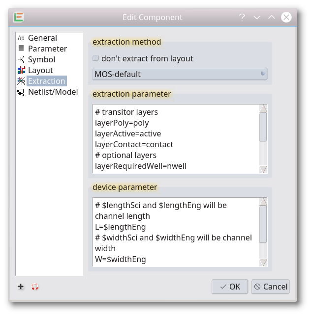
Layout describes how to build layout from the schematic. Extraction describes the opposite: how to recognize a device in layout when schematic properties are missing (for example after a clean layout-only delivery).
Devices placed by schematic-driven layout can often be recognized anyway, because LayoutEditor stores component information on the cell reference. Filling this tab is for stronger layout-vs-schematic checks and parasitic-style extraction.
Fields:
- whether extraction is used at all
- method (for example plate capacitor, thin-film resistor, MOS, BJT variants)
- parameters for the method (layers, ports, coefficients, …)
- parameters written back to the extracted device
Built-in method names include for example C-parallelPlate, C-nodeToGround, R-thinFilm, MOS-default, BJT-lateral, BJT-vertical. Each method has its own parameter template in the dialog—read the comments in those templates carefully; they explain the required layers and ports in place.
Netlist / Model
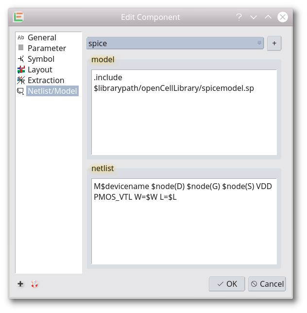
Here you define how the device appears in a simulation netlist.
For each format name (for example spice, hspice, spectre):
- Netlist — one contribution per placed instance (the device line)
- Model — text emitted once per component type (models, subcircuits, …)
Netlist generation setups pull these pieces in with commands such as $netlist(format) and $model(format). See the netlist chapters and the examples shipped with the SchematicEditor.
Common placeholders in the netlist text:
$devicename— instance name$node(portName)— the net connected to that symbol port$value/$parameterName— parameter values
Create netlist/model information from schematic
For hierarchical / internal (and some OA) components, you can enable create netlist/model information from schematic. Then LayoutEditor builds the hierarchical netlist/model from the sheet that defines the component, instead of you typing the subcircuit by hand. Manual netlist/model fields are then driven by that generation path.
Import and Delete (after pressing +)
Import
Import fills the dialog from another source, for example:
- LayoutEditor
.lel - LTspice
.asy - xschem
.sym - Qucs / Eagle / KiCad libraries
- OpenAccess
Foreign formats often bring a good symbol and some parameters, but may miss layout recipes, full netlist templates, or LayoutEditor-only options. After import, complete the missing tabs and save into a .lel library so everything is stored in the native format that supports all options.
Delete
Removes the component from the library file. Devices already placed in open schematics can remain usable in memory, but new placements from that library entry will no longer work after reload—so use Delete carefully.
Practical checklist for a solid component
- Clear name, prefix, and description
- Symbol with correct ports
- Parameters users need (with units/info; formulas only where useful)
- Layout method that matches your flow (fixed cell, package, macro, Tcl/Magic, gdsFactory, OA, …)
- Netlist/Model for the simulators you use
- Save in a writable
.lel(and maintain library Info / filters for the whole kit)
If you maintain a PDK, treat the .lel library as the master definition: schematics (LES) only place and wire these components; they should not quietly become a second incomplete copy of the library.
© 2026 juspertor GmbH