Netlist
All netlist tools are loaced in the netlist window. This window can be opened by a right click in an empty area of the toolbar and marking the netlist in the window list. Also these tools will be opened in case the SchematicEditor is opened. Furthermore some netlist tools are part of the Utilities menu.
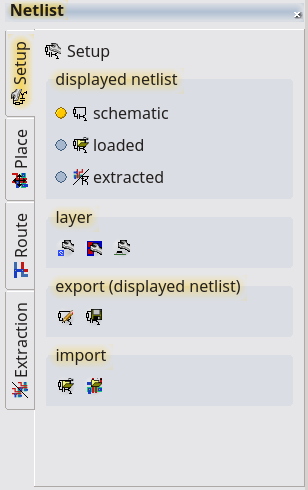
Netlist Basics
The LayoutEditor can have up to 3 netlists for any cell of the deisgn. The netlists are separated by origin. A netlist for any cell can be loaded from a netlist file, taken from the SchematicEditor, or be extracted from the cell. Each of these netlists can be viewed with the TextEditor in any supported netlist format and stored to disk. How netlists are created is part of the SchematicEditor documentation.
Loading Netlists
The load feature is loaced in the setup tab of the netlist tool and in the Utilities menu. Supported formats are: spice, structual VHDL, alliance, qucs, eagle, PADSpcb and OpenAccess. Support for other file format can be extended on request. Most netlist formats refer to the devices by a name. To link this name to a physical device layout, the device names can be searched in the libraries of the SchematicEditor and in additional netlist import libraries. These import libraries can be setup with the Add Library feature located next to the Import Netlist feature in the netlists tool. SchematicEditor Libraries can be setup in the SchematicEditor.
Netlist Import Libraries
Supported formats are: Alliance, LayoutEditor Library (file extension '.lel'). The LayoutEditor Library Format is a simple text file. Lines starting with a '#' are comments. The library is split into five sections ('cell','macro','package','parts','ignore'). Each section starts with the section name in bracets ('[..]'). Here is an example LayoutEditor library file with explanations:
# LayoutEditor Library file
# Section cell: all matching elements are linked to an existing cell<
[cell]
# format:
# device-type layout-file cellname pins
MOPEN microwavelib.gds MOPEN pin1
'MSTEP W1="2 mm" W2="0.244 mm"' microwavelib.gds MSTEP2000_244 pin1 pin2
'MTEE W1="0.244 mm"' microwavelib.gds MTEE244 pin1 pin2 pin3
# If a device has parameters or the device name has spaces, put the device name in
# single or double quotes.
# Additionals parameters are ignored in the search.
# So in this example MOPEN will match for any parameter.
# Section macro: a macro is call, which generates the required cell.
[macro]
# format:
# device-type macro-file pins
MLIN microstrip.layout pin1 pin2
# The macro must set the new cell to the currentCell to be recognized.
# Some #DEFINES are made in the macros:
# NETLIST_PARAMETER, NETLIST_DEVICENAME, NETLIST_PIN1_NAME
# Section package: all matching elements are linked to an cell.
# cellname, pin name, pin number and devicename is set
# Matches to all devices containing the package-type
[package]
# format:
# package-type layout-file cellname pin name,pin number ...
LT1028 DIP8.gds DIP8 in+ 3 in- 2 V+ 7 V- 4 out 6
#Section ignore: all matching elements are removed from the netlist
[ignore]
SUBST
Pac
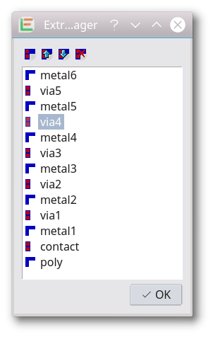
EqnRouting Layers
This feature is used to route the connection in a layout, or to extract netlist highlighting and connectivity information. There are different ways to enter this information. All setup features are located in the setup tab of the netlist-tools.
Layer Manager
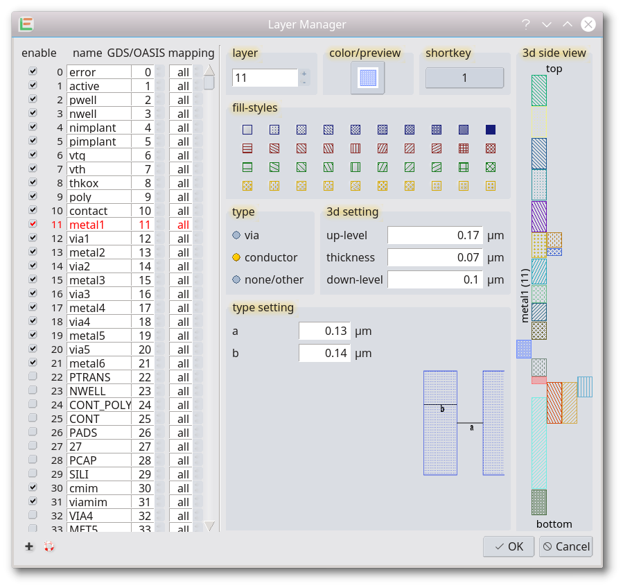 The layer manager can tell you if the layer is a connecting layer, a via layer, or has no connecting feature. Technology information like minimum width and minimum spacing can be set. The order of the layers is set by its 3d settings.
Import from File
Inside the Layer Manager there is a feature Import Layer Settings (visible after pressing the litte + in the lower left). This feature will load all layer settings from a file, it includes the connecting information. Connecting information is not included in all supported layer files.
Layer Stack
 Identical information can be set to Layer Stack which is an alternative way to enter the data. Clicking on one layer will show the technology data for that layer.
PCB Layer Setup
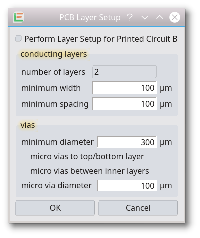 An assistance setup dialog is available for Printed Circuit Boards (PCB). This layer setup is mandatory in use with several PCB file formats.
Macros
All the required setups can of course also be done with a macro. Any layer setup macro generated by its feature in the Layer Manager (visible after pressing the little + in the lower left of the Layer Manager) includes also the connecting information. For example, with the technology OpenCellLibrary, a layer setup macro is located under Utilities/Technology/OpenCellLibrary.
© 2026 juspertor GmbH